Notes about fault finding in a subtly broken Yamaha TX802.
Conclusion: problem solved by replacing the EGM IC.
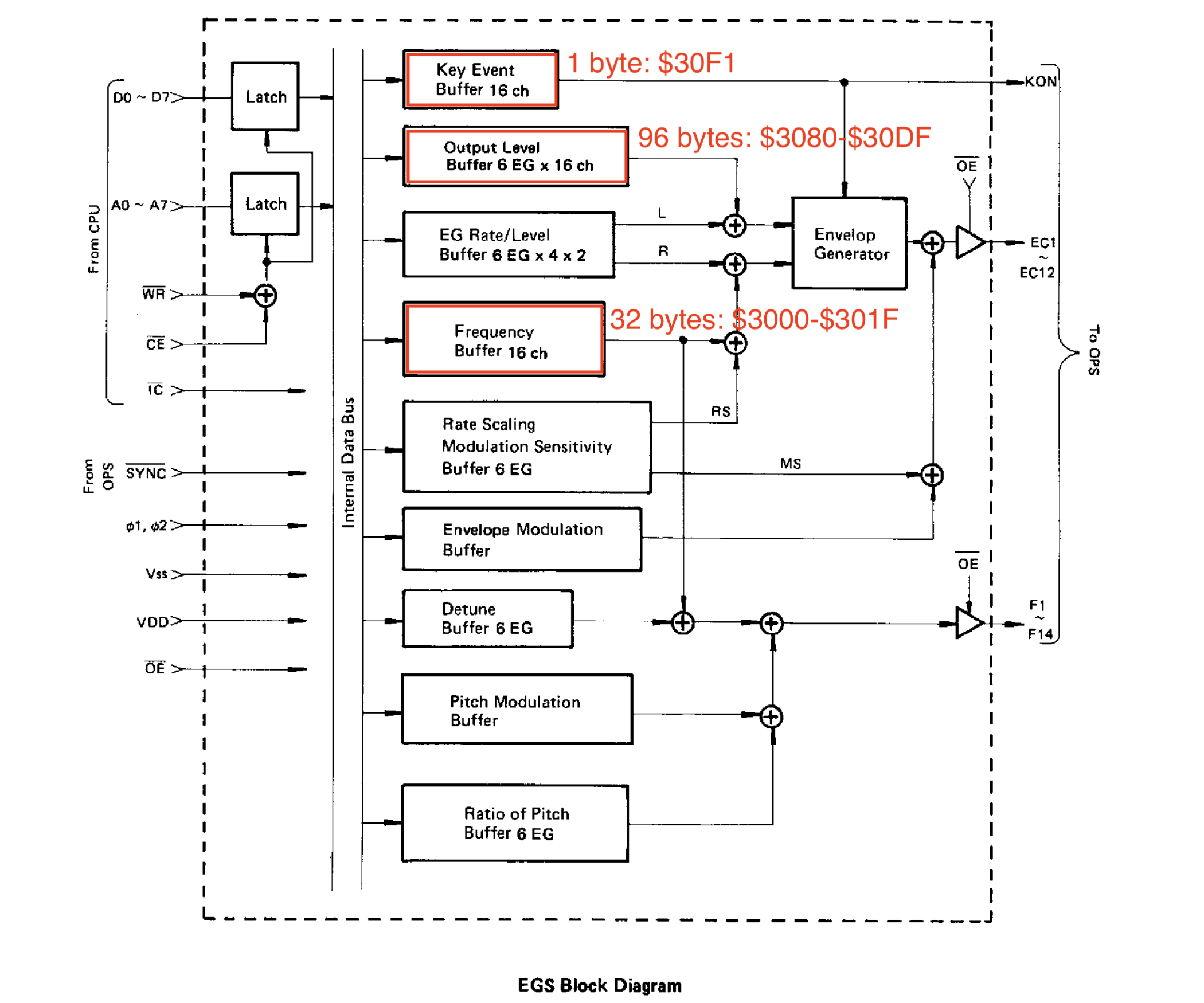
The EGS and OPS ASICs of the DX7 are well-studied. Much less is known (or easy to find) about the DX7II/TX802 and their EGM/OPS2 ASIC pair.
One of the big questions is whether the fault is in the EGM or before the EGM. To decide this we need to understand how the EGM works.
Relevant paragraphs in the patent:
Interesting points:
Not clear which points apply to the EGS. The EGS and OPS are not recognizable in the block diagrams of the patent. The interface of the EGS does not appear to require constant refresh of parameters.
What data must flow from CPU to EGS? The ajxs ROM disassembly answers this question, and this is consistent with the DX7/9 service manual block diagram. The key insight is that the DX7 is monotimbral. Even though the OPS is multi-timbral, the EGS is not. Its 8-bit wide address space can be divided into global parameters and per-voice parameters. The per-voice parameters use 129 bytes of address space.
The EGM cannot use the same interface design because it is at least 8-part multi-timbral, if not 16-part.
I've started to disassemble the firmware of the secondary CPU (which drives the sound generator ASICs) using f9dasm.
It's not very readable but you can see the current state of the disassembly here.
| Disassembly name | Address | Width | Accessed from | Guess |
|---|---|---|---|---|
| EGM_00 | $1000-?? | 8,16 | main loop | Operator parameters |
| $1010-$1015 | 8 | ? | Operator output levels (OP6-OP1), written at note on. Level 0 is 0xff, level 99 is 0xf0. | |
| EGM_16 | $1016 | 8 | main loop | Note on/off |
| EGM_17 | $1017 | 8 | timer, main loop | Voice select. Values: 0x00-0x0f, 0x1f, 0x3f, 0x5f, 0x7f, 0x9f, 0xbf, 0xdf, 0xff |
| EGM_18 | $1018 | 16 | timer, main loop | Voice param |
| EGM_1A | $101A | 16 | timer, main loop | Voice param |
| EGM_1C | $101C | 16 | timer | Voice LFO |
| EGM_1F | $101F | 8 | main init | Reset |
The secondary CPU emits a bus synchronization signal called 'E' that allows peripherals to time reads and writes. The phi1 and phi2 clocks used by EGM/OPS2 are in turn synchronized to the E clock. This appears to be the purpose of XOR gate IC66. Even though phi1 and phi2 run twice as fast as E, they are aligned.
The aligned phi1 and phi2 clocks then pass through what the TX7 schematic calls a "Duty Converter" circuit which uses an AND gate IC28 and a RC lowpass to create a time-delayed pulse. For phi2 the end result looks like this, where the yellow CH1 is E and blue CH2 is phi2. Note that the frequency of phi2 is twice that of E, and phi2 is delayed.
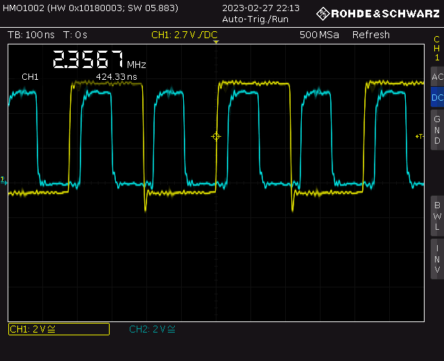
I have no reason to believe the phi2 delay is off because it is the same as the phi1 delay, which uses the same lowpass and AND gate trick.
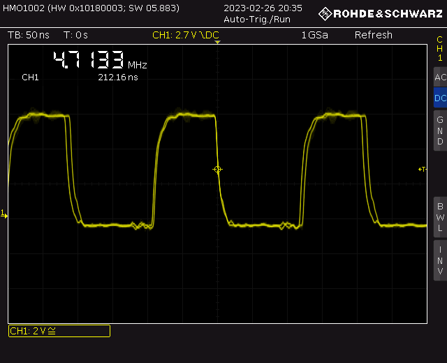
There is a weird looking jitter when you look at the phi2 clock in isolation.
The jitter starts appearing from IC66 (XOR) pin 3 onwards. I suspect it is a side effect of the synchronization.
When E is low, the /CE2 line of the EGM is high because of how the E clock connects to the IC25 decoder. This means that from a bus access perspective, the EGM will ignore the phi2 pulse while E is low. The timing diagram in the HD6303 service manual suggests that some fixed time after E goes high, both the address and the data for a write are loaded.
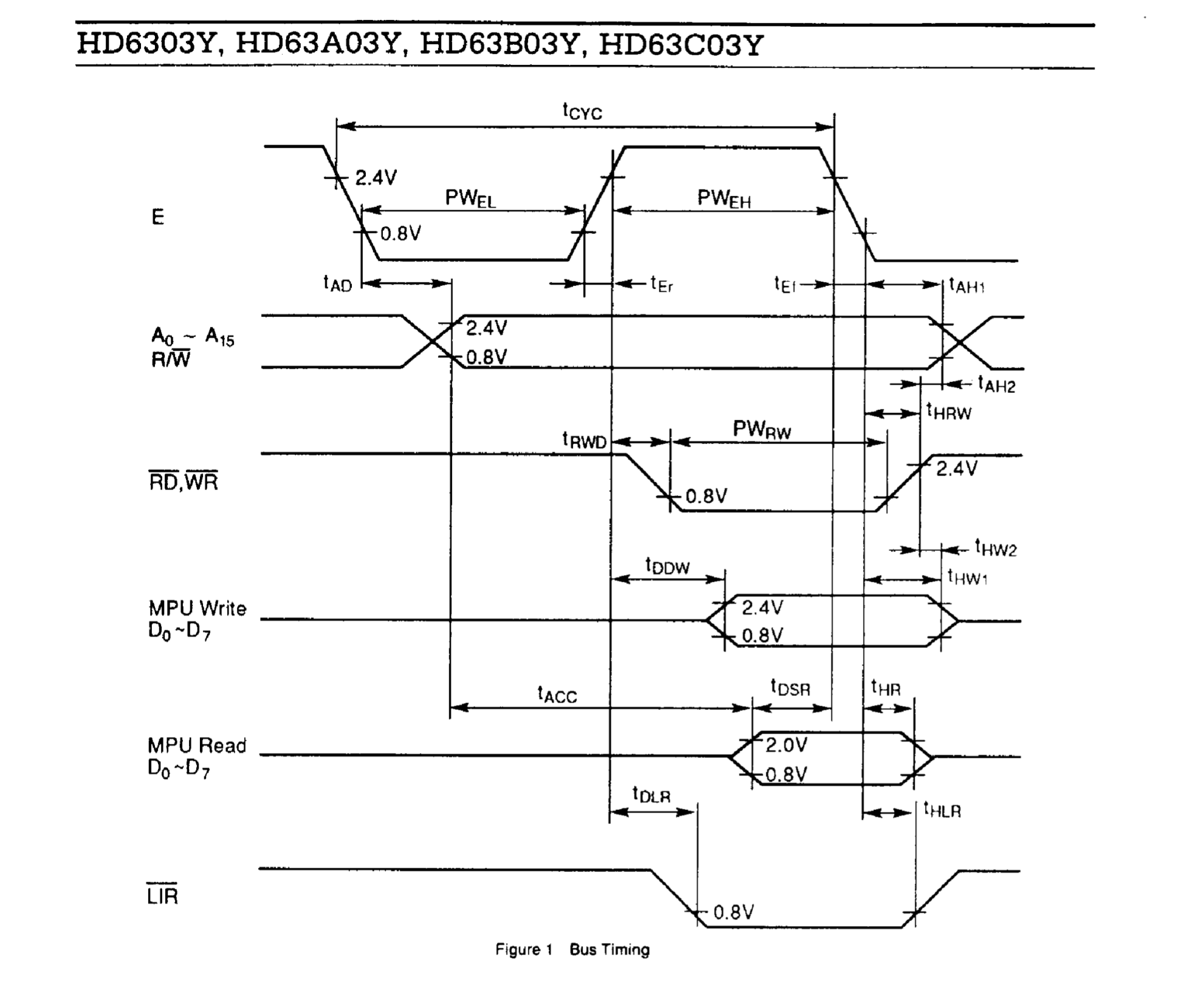
My guess is that the delay of the phi2 clock is chosen so that the falling edge of phi2 happens when the write data is present. Consider the following capture from the logic analyzer, captured at 50MHz. The E clock is unfortunately missing from the capture.
 A   D /CE1 /CE2 phi2
03  17   0    1    1  # Leftover address and data from previous tick
03  17   0    1    1
17  17   0    1    1  # MPU sends address 0x17 while E low
17  17   0    1    1
17  17   0    1    1
17  17   0    1    0  # phi2 falling edge but data ignored by EGM
17  17   0    1    0  # since /CE2 is high.
17  17   0    1    0
17  17   0    1    0
17  17   0    1    0  # (approx) E goes high
17  17   0    0    0
17  17   0    1    1  # phi2 goes high. Odd: /CE2 flaps to 1
17  00   0    0    1  # MPU sends data 0x00
17  00   0    0    1
17  00   0    0    1
17  00   0    0    1
17  00   0    0    0  # falling edge of phi2, both CE lines low,
17  00   0    0    0  # EGM reads data 0x0 at address 0x17
17  00   0    0    0
17  00   0    0    0
17  00   0    1    0
17  00   0    1    0
What happens at key on?
What must happen when?
Ken Shirriff notes that the "A register" of the OPS holds 16 algorithm values. The same must be true for the OPS2, because CPU2 is unable to send each algorithm to the OPS2 on time the way pitch and amplitude words are delivered.
Music-synthesizer-for-android is a DX7 reverse engineering project by Raph Levien.
There are interesting pieces of information scattered around this repository.
The interface works normally, but the sound coming out the outputs does not match the parameter values in the interface.
All observations indicate that OPS2 works correctly. It can produce audio output with varying pitch, loudness and FM algorithms. It receives correct inputs and produces correct outputs.
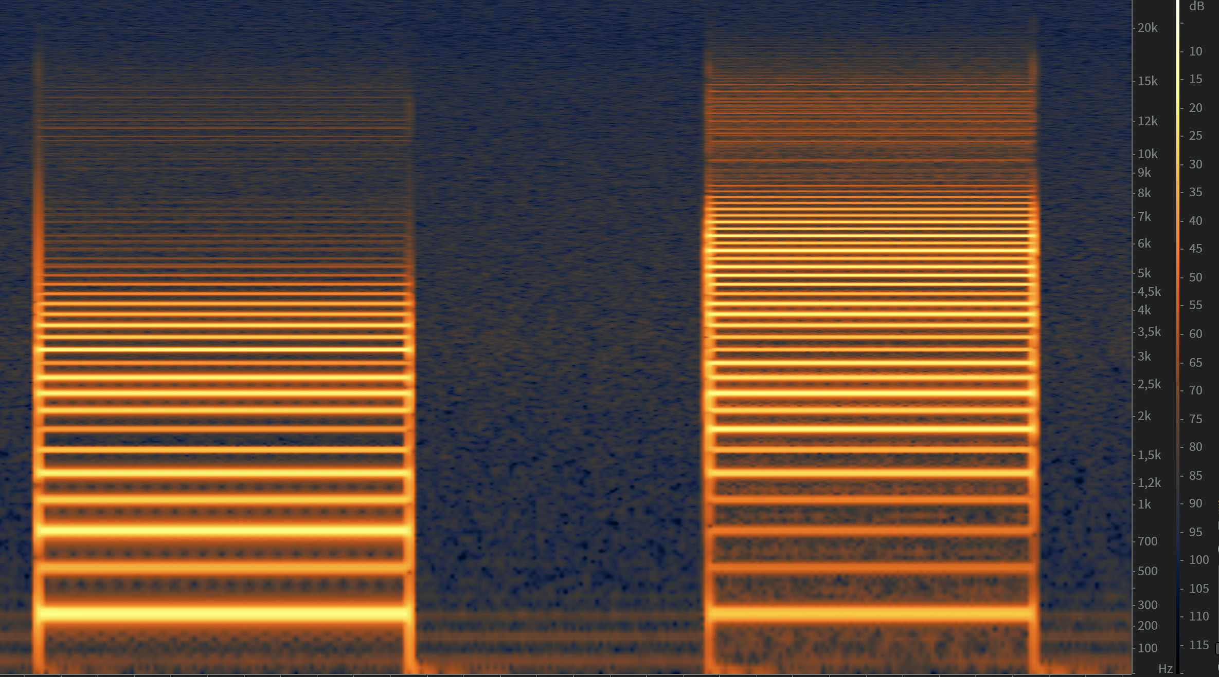
At first glance it seems all operators are pegged at the maximum output level (99). Listening closer, you hear that the output levels are higher than 99.
The following recording plays:
Looking at a spectrum visualization, you clearly see that the harmonics line up, but that the harmonics from the TX802 are louder.
Even though envelope levels L1, L2 and L3 are ignored, Amplitude Modulation Sensitivity (AMS) works correctly. Consider the following recording.
Note that Ams 7 "wins" from the pegged output level: there is no output from OP2 until I move the mod wheel.